Loading
Electronics Manufacturing
For Telecom Infrastructure
That Can’t Go Down
We manufacture high-density PCB assemblies, cable harnesses, and integrated systems built for the reliability and signal integrity that telecom infrastructure demands.
What telecom electronics manufacturing
actually demands
Telecom buyers evaluate EMS partners on reliability, technical depth, and speed. These are the challenges that separate a
genuinely telecom-capable manufacturer from one adapting a generic process.
Challenge  01
Uptime is everything, failure has immediate impact
A failed PCB in a base station or switching system means network downtime directly impacting end users and operator SLAs. Telecom electronics require near-zero defect rates and proven reliability before deployment.
01
Uptime is everything, failure has immediate impact
A failed PCB in a base station or switching system means network downtime directly impacting end users and operator SLAs. Telecom electronics require near-zero defect rates and proven reliability before deployment.
Challenge  02
High-density designs with signal integrity demands
Telecom PCBs are among the most complex in electronics - high-density, high-speed, with tight signal integrity requirements. Assembly errors at fine-pitch components or BGAs can corrupt performance in ways that aren't immediately visible.
02
High-density designs with signal integrity demands
Telecom PCBs are among the most complex in electronics - high-density, high-speed, with tight signal integrity requirements. Assembly errors at fine-pitch components or BGAs can corrupt performance in ways that aren't immediately visible.
Challenge  03
Rapid technology cycles requiring fast NPI
Telecom technology evolves fast from 4G to 5G, edge computing, Open RAN. New products need to reach market quickly without sacrificing the validation rigour that network operators demand before deployment.
03
Rapid technology cycles requiring fast NPI
Telecom technology evolves fast from 4G to 5G, edge computing, Open RAN. New products need to reach market quickly without sacrificing the validation rigour that network operators demand before deployment.
Challenge  04
Volume variation across product generations
Telecom programmes often ramp fast and wind down as technology transitions. Manufacturers need flexibility to scale production up and down without quality or lead time penalties at either end.
04
Volume variation across product generations
Telecom programmes often ramp fast and wind down as technology transitions. Manufacturers need flexibility to scale production up and down without quality or lead time penalties at either end.
Manufacturing solutions built for telecom's demands.
Every service we provide to telecom clients is configured for the reliability, signal integrity, and speed
requirements of communications infrastructure not adapted from a consumer electronics process.


Fine-pitch SMT, BGA, and mixed-technology assembly for complex telecom boards - 100% AOI, X-ray on all BGA joints, and ICT ensuring signal integrity and assembly quality across every unit.

Shielded cables, high-speed data cables, and power harnesses built and tested for signal integrity and reliability for rack, outdoor, and field-deployed network equipment.

End-to-end functional testing, burn-in, and boundary scan for high-density telecom assemblies verifying performance under real operating conditions before units enter network deployment.

24–72h quick-turn prototype capability and dedicated NPI resource enabling telecom OEMs to validate new products and reach production quickly across fast-moving technology generations.

Complete network equipment integration - PCBs, cable harnesses, and enclosures assembled into a fully tested, deployment-ready system under one roof.

DFM review focused on signal integrity, thermal management, test point placement, and BGA accessibility catching design risks that affect telecom performance before the first prototype is built.
High-density PCB assembly
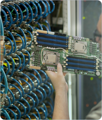
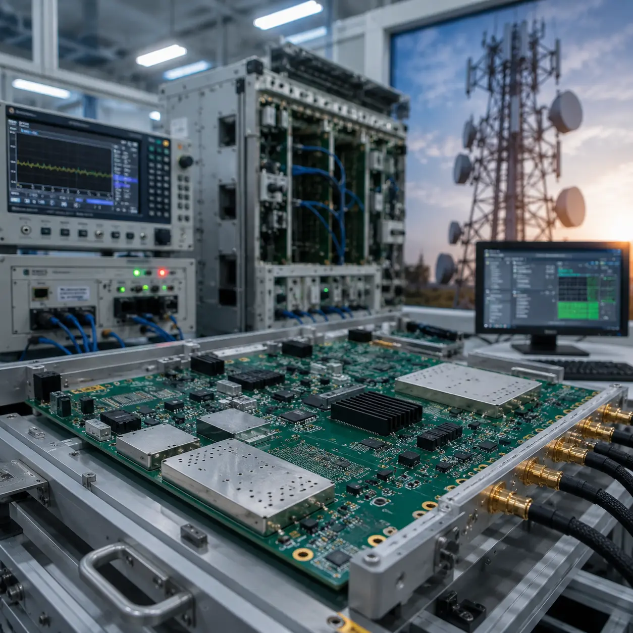
Fine-pitch SMT, BGA, and mixed-technology assembly for complex telecom boards - 100% AOI, X-ray on all BGA joints, and ICT ensuring signal integrity and assembly quality across every unit.
Cable harness for network infrastructure
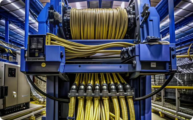
Shielded cables, high-speed data cables, and power harnesses built and tested for signal integrity and reliability for rack, outdoor, and field-deployed network equipment.
Functional & boundary scan testing
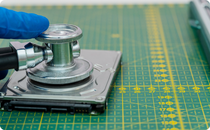
End-to-end functional testing, burn-in, and boundary scan for high-density telecom assemblies verifying performance under real operating conditions before units enter network deployment.
Fast-turn NPI for rapid technology cycles
24–72h quick-turn prototype capability and dedicated NPI resource enabling telecom OEMs to validate new products and reach production quickly across fast-moving technology generations.
Box build & system integration
Complete network equipment integration - PCBs, cable harnesses, and enclosures assembled into a fully tested, deployment-ready system under one roof.
DFM for high-density telecom designs
DFM review focused on signal integrity, thermal management, test point placement, and BGA accessibility catching design risks that affect telecom performance before the first prototype is built.
The standards that underpin telecom
electronics manufacturing
Every telecom programme with us is aligned to the workmanship, testing, and compliance
standards that network operators and equipment certification bodies require.
IPC-A-610 Class 2 & 3
Class 2 for commercial telecom builds, Class 3 for mission-critical infrastructure, the workmanship quality and inspection rigour that network reliability demands.
X-ray & boundary scan inspection
X-ray on all BGA joints and boundary scan for high-density boards providing hidden joint and interconnect verification that complex telecom assemblies require.
RoHS & REACH compliance
All telecom assemblies built to RoHS and REACH compliance meeting the environmental requirements of global telecom equipment markets.
ISO 9001 certified QMS
Certified quality management system providing the process discipline and documentation control that telecom OEM supply chains require from their manufacturing partners.
Why telecom teams choose us
Network equipment must work first time, every time. Here’s what makes us the right manufacturing
partner for telecom programmes where reliability is non-negotiable.
High-density assembly capability
Fine-pitch, BGA, and multi-layer board assembly with X-ray verification and boundary scan, the technical depth telecom’s most complex PCBs require to perform reliably in network environments.
Fast NPI for rapid technology cycles
24–72h prototype turnaround and dedicated NPI resource so new telecom products move from design to validated pilot without the delays that cost market position in fast-moving technology generations.
PCB assembly + cable harness under one roof
Boards and cables built by the same team eliminating the coordination and traceability gaps that come with managing separate PCB and cable assembly suppliers for network equipment programmes.
Scalable production for volume variation
Flexible lines that scale from prototype to high-volume and back without quality or lead time penalties as technology generations come and go across your product portfolio.
Burn-in and stress screening as standard
Every telecom assembly subjected to burn-in and environmental stress screening before despatch catching infant mortality failures before they reach a network deployment where downtime costs are significant.
25+ years of electronics manufacturing experience
Cross-industry manufacturing depth that brings production discipline, supply chain resilience, and quality systems built for the reliability standards telecom infrastructure demands.
Why telecom teams choose us
Network equipment must work first time, every time. Here’s what makes us the right manufacturing
partner for telecom programmes where reliability is non-negotiable.
5G base station PCB assembly — zero field failures
across initial network deployment batch
Problem
A telecom OEM launching a new 5G base station module needed high-density BGA PCB assembly with signal integrity verification and functional testing on a compressed timeline to meet network operator deployment commitments.
Solution
We configured a dedicated line with 100% X-ray on all BGA joints, boundary scan testing, ICT, and full functional test completing NPI to production-ready in 8 weeks with test coverage designed for the specific signal paths of the board.
Outcome
Zero field failures across the initial deployment batch. Client met network operator deployment deadline. Programme scaled to full volume within 3 months of first production release.
0 field failures · 8-week NPI · on-time deployment
Ready to discuss your telecom programme?
Tell us about your product and network deployment requirements and our team responds within 24 hours.